


Device Research Laboratory (DRL)
Block No.4, Room No. 402A, ECE Dept, MAIT
Thrust Areas
- Compact Modelling Of Gate All Around (GAA) MOSFET.
- Research of Innovative Device Architectures.
- Reliability Analysis of MOSFET under stressful conditions.
- Device Applications for various purposes.
Latest Device Architectures

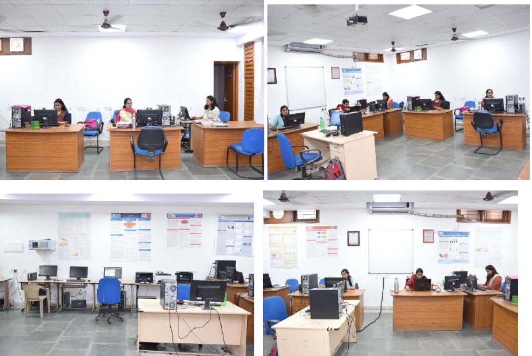
The Device Research Laboratory (DRL) in the department of Electronics and Communication (ECE) is well equipped. It has two advanced servers and 8 computer system with latest configuration. In addition to all this there is one colour and two normal printers. There are two advanced simulators, one is Silvaco ATLAS 3D device simulator and the other one is Visual TCAD device simulator. The students are working on various devices such as:- Junctionless Double Surrounding Gate (JLDSG) MOSFET, Gate Engineered Gate Stack Schottky Barrier Gate All Around MOSFET and Junctionless Accumulation Mode Cylindrical Surrounding Gate MOSFET. Also at present there is one DRDO project entitled "Analysis and Characterization of Silicon Gate All Around (GAA) nanowire MOSFET for ULSI circuit applications". In 2015 about 12 papers were published in International Journal and Conferences. In 2016 till 31st March7 have been published in International Journals and Conferences. Some Latest publications have been listed below.
Latest Publications
Patents
- Neelam Sharma, Patent number-542328, titled “Load Sensing Module for load Machines” Date of Grant: June 20, 2024.
- Neelam Sharma, Madan Lal Sharma, Vasudha Bahl, Soumi Ghosh, Pooja Gupta, Ajak Kumar, Krishna Chandra Tripathi, Abhishek Yadav, Patent number-202024105921, titled “Intuitive Air Gesture Recognition System for Dynamic Computer Interaction Using Machine Learning” Date of Grant: November 12, 2024.
- Anubha Goel, Sonam Rewari, Seema Verma and R.S. Gupta, Patent number-391269, titled “Nanotube FET BIOSENSOR System and Method for Detection of DNA and Biomolecules Using the same", dated June 26, 2019, Date of Grant: March 7, 2022.
- Shalu Garg, Anubha Goel, Jasdeep Kaur, Subhasis Haldar, R.S. Gupta, Neeraj, S. S. Deswal, Patent number- 202511015533, titled “A system to monitor cell growth” Published.
- Neeraj, Anubha Goel, Shobha Sharma, Subhasis Haldar, R.S. Gupta, Shalu Garg, S. S. Deswal, Patent number-202311053897, titled “A Field Effect Transistor for Detecting GAS” Published.
Copyrights
- Shalu Garg, Anubha Goel, Jasdeep Kaur, Subhasis Haldar, R.S. Gupta, Diary No.: 13014/2023-CO/SW, titled “Physics based analytical modeling and simulation No of Cylindrical Junctionless Nanowire Ferroelectric Field Effect Transistor (CJNFe-FET) for enhanced analog performance”, dated January 18, 2024, ROC NO.: SW-18133/2024.
- Shalu Garg, Anubha Goel, Jasdeep Kaur, R.S. Gupta, Diary No.: 2941/2023-CO/SW, titled “Temperature sensitive analysis of Junctionless Nanowire Ferroelectric Field Effect Transistor (JNFe-FET) for enhanced analog performance”, dated October 31, 2023, ROC NO.: SW-17480/2023.
- Neeraj, Anubha Goel, Shobha Sharma, R.S. Gupta, Diary No.: 10220/2023-CO/SW, titled “Sic based analytical model for gate-stack dual metal nanowire fet for enhanced analog performance”, dated June 16, 2023, ROC NO.: SW-16636/2023.
- Neeraj, Anubha Goel, Shobha Sharma, R.S. Gupta, Diary No.: 10219/2023-CO/SW, titled “Temperature sensitive analytical analysis of gate stack dual-metal nanowire field effect transistor (4h-sic)”, dated November 15, 2023, ROC NO.: SW-17592/2023.
- Swati Sharma, Vandana Nath, S.S. Deswal, R.S. Gupta, Diary No.: 10828/2024-CO/SW, titled “GALLIUM NITRIDE BASED SCHOTTKY BARRIER MOSFET BIOSENSOR”, dated December 04, 2024, ROC NO.: SW-19790/2024.
- Swati Sharma, Preeti Goyal, Vandana Nath, S.S. Deswal, R.S. Gupta, Diary No.: 11687/2024-CO/SW, titled “GALLIUM NITRIDE BASED HIGH-K SCHOTTKY BARRIER MOSFET BIOSENSOR”, dated December 04, 2024, ROC NO.: SW-19796/2024.
Papers in Reviewed Journal (Published)
- Anubha Goel, Sonam Rewari, R.S. Gupta, “Performance investigation of neoteric Pt/Pd Junctionless gas tube FET(JL-GT-FET) as a Hydrogen(H2) gas sensor for industrial applications-analytical model Extraction of Non-Quasi-Static Model Parameters for Cylindrical Gate-Stacked Junction-less Accumulation Mode MOSFET and Its Implementation as RF Filters for Circuit Applications” Micro and Nanostructures Journal (Elsevier), Volume: 198, pp 208050, Feb 2025. (Print ISSN: 2773-0123, Digital Object Identifier: 1016/j.micrna.2024.208050, Impact Factor: 3.0).
- Jitender Kumar, Amit Saxena, S. S. Deswal, Aparna N. Mahajan, R.S. Gupta, “Analytical modeling of cylindrical Silicon-on-Insulator Schottky Barrier MOSFET and impact of insulator pillar radius on analog/RF and linearity parameters for low power circuit application” Microelectronics Journal, Volume: 156, pp 106505, Feb 2025. (Print ISSN: 1879-2391, Digital Object Identifier: 1016/j.mejo.2024.106505Get rights and content, Impact Factor: 2.3).
- Shalu Garg, Jasdeep Kaur, Anubha Goel, Subhasis Haldar, R.S. Gupta, “Accurate 2-D Analytical Model for Cylindrical Gate- Junctionless Ferrolectric Nanowire (CG-JFe- FET) MOSFET with Scaled Channel Length” Physica Scripta, Volume: 99, Issue: 5, pp 055240, Apr 2024. (Print ISSN: 1402-4896, Digital Object Identifier: 1088/1402-4896/ad39b9, Impact Factor: 2.6).
- Shalu Garg, Jasdeep Kaur, Anubha Goel, Subhasis Haldar, R.S. Gupta, “Dielectric Pocket Engineered, Gate Induced Drain Leakages (GIDL) and Analog Performance Analysis of Dual Metal Nanowire Ferroelectric MOSFET (DPE-DM-NW-Fe FET) as an Inverter” Microsystem Technologies, Volume: 31, Issue: 2, pp 581-592, Apr 2024. (Print ISSN: 9467076, Digital Object Identifier: 1088/1402-4896/ad39b9, Impact Factor: 2.6).
- Neeraj, Shobha Sharma, Anubha Goel, Sonam Rewari, S.S. Deswal, S. Gupta, “Impact of Interface Trap Charges on Silicon Carbide (4H-SiC) Based Gate – Stack, Dual Metal, Surrounding Gate, FET (4H-SiC- GSDM-SGFET) for Analog and Noise Performance Analysis for 5G/LTE Applications” ECS Journal of Solid State Science and Technology, Volume: 13, Issue: 7, pp 073015, July 2024. (Print ISSN: 2162-8777, Digital Object Identifier: 10.1149/2162-8777/ad26a2, Impact Factor: 2.2).
- Neeraj, Shobha Sharma, Anubha Goel, Sonam Rewari, S.S. Deswal, S. Gupta, “Modeling and Simulation Characteristics of a Highly-Sensitive Stack-Engineered Junctionless Accumulation Nanowire FET for PH3 Gas Detection” ECS Journal of Solid-State Science and Technology, Volume: 13, Issue: 2, pp 027007, Feb 2024. (Print ISSN: 2162-8777, Digital Object Identifier: 10.1149/2162-8777/ad26a2, Impact Factor: 2.2).
- Ajay Kumar Gupta, Manav R. Bhatnagar, “A Non-Cooperative Pricing Strategy for UAV-Enabled Charging of Wireless Sensor Network” IEEE Transaction on Green Communication and Networking, July 2024. (Print ISSN: 2473-2400, Digital Object Identifier: 1109/TGCN.2024.3434603, Impact Factor: 6.7).
- Ajay Kumar Gupta, Manav R. Bhatnagar, “St-Hot: A Prospect of Price Equilibrium in a Multi-player Game for Electric Vehicle Charging Application” IEEE Access, July 2024. (Print ISSN: 21693536, Digital Object Identifier: 1109/ACCESS.2024.3435367, Impact Factor: 3.6).
- Swati Sharma, Vandana Nath, S. Deswal, R.S. Gupta, “Analytical modelling and sensitivity analysis of Gallium Nitride-Gate Material and, dielectric engineered- Schottky nano-wire fet (GaN-GME-DE-SNW-fet) based label-free biosensor” Microelectronics Journal, Volume: 129, pp 105599, Sept 2022. (Print ISSN: 9598324, Digital Object Identifier: 10.1016/j.mejo.2022.105599, Impact Factor: 2.3).
- Sumeda Gupta, Neeta Pandey, S. Gupta, “Analytical model for junctionless accumulation‐mode cylindrical surrounding gate (JAM‐CSG) MOSFET as a biosensor” International Journal of Numerical Modelling, Volume: 36, Issue: 5 pp e3095, Sep 2023. (Print ISSN: 1099-1204, Digital Object Identifier: 10.1002/jnm.3095, Impact Factor: 2.39)